Third-order optical nonlinearity, concerning both nonlinear absorption (NLA) and nonlinear refraction (NLR), is becoming an important parameter to evaluate the potential applications of materials in a number of fields, such as integrated optics, optical switching devices, and optical signal processing. The imaginary (Imχ(3)) and real (Reχ(3)) parts of the third-order nonlinear susceptibility (χ(3)) are usually evaluated through the nonlinear absorption coefficient (βeff) and the nonlinear refractive index (n2). The nonlinear refractive index n2 in some conventional crystals, semiconductors, one-dimensional (1D) and two-dimensional (2D) nanomaterials have attracted much attention in the nonlinear optical properties investigation. In parallel, the search for pristine transition metal dichalcogenides has not been adequately exploited.
Researchers in Prof. Jun Wang’s group from Shanghai Institute of Optics and Fine Mechanics, Chinese Academy of Sciences, have investigated the nonlinear absorption and refractive properties of these 2D WS2 and WSe2 semiconductor films with different thicknesses, including monolayer and multilayer, by using Z-scan technique with femtosecond pulses at the wavelength of 1040 nm. It displays that these semiconductor films have two-photon-absorption (TPA) induced optical limiting performances, and the third-order nonlinear optical parameters βeff, Imχ(3), n2, and Reχ(3) decrease as the sample thickness increases. In addition, the monolayer WS2 film possesses a positive n2 of ~1.28 × 10?10 cm2 W?1, while it is negative with the values of ~10?12 cm2 W?1 in these thicker WS2 films. This can be qualitatively discussed based on the band structure, strong excitonic effect, nonlinear refraction dispersion, bandgap scaling associated with TPA, etc.
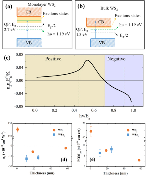
It has been demonstrated that WS2 will transform from an indirect optical bandgap (~1.3 eV) to a direct optical bandgap (~2.05 eV) semiconductor when the bulk crystal is sliced down to the monolayer. As the excitation photon energy is ~1.19 eV, the TPA effect can occur both in the monolayer and thicker WS2 samples. Ye et al. have demonstrated that the dark excitonic absorption will significantly enhance the TPA in monolayer WS2 [1]. As shown in Fig. 1, monolayer WS2 has a direct band structure with the quasiparticle bandgap (Eg) of ~2.7 eV and the excitonic binding energy as large as ~0.7 eV from the excitonic ground state (corresponding to the optical bandgap ~2.05 eV). Therefore, the TPA process is located in the interior of these exciton states and produces strong dark exciton resonance absorption. However, as for bulk WS2, the excitonic binding energy is lower than one-tenth of the value in monolayer WS2 [2]. The strong excitonic resonance absorption is a probable reason for the fact that WS2 exhibits a larger βeff when thinned down to the monolayer. On the other hand, Sheik-Bahae et al. have carried out very in-depth research on the behavior of the dispersion of n2 associated with TPA [3]. They found that if hυ < Eg, the n2 will change from positive to negative when the excitation energy moves from the lower frequency side of the TPA edge (Eg∕2) to the higher side due to the n2 dispersion during the TPA process in semiconductors [Fig. 1(c)]. The green line and blue line correspond to the hυ/Eg values of the monolayer and bulk WS2 in our experiment, respectively. This is consistent with our result as the sign of n2 for monolayer WS2 (~0.75 nm) is positive, while it is negative for ~18.8 and 54.9 nm WS2 because the hυ/Eg for the monolayer is 0.44, while it is 0.92 for bulk [Fig. 1(d)].
This study was published on Optics Letters on Aug. 13, 2016. [https://www.osapublishing.org/ol/abstract.cfm?uri=ol-41-17-3936&origin=search]
This work was supported by the Chinese National Natural Science Foundation, the External Cooperation Program of BIC, CAS, and the Excellent Academic Leader of Shanghai.
References:
1. Z. L. Ye, T. Cao, K. O’Brien, H. Y. Zhu, X. B. Yin, Y. Wang, S. G. Louie, and X. Zhang, Nature 513, 214 (2014).
2. A. R. Beal, J. C. Knights, and W. Y. Liang, J. Phys. C 5, 3540 (1972).
3. M. Sheik-Bahae, D. J. Hagan, and E. W. Van Stryland, Phys. Rev. Lett. 65, 96 (1990).

Fig. 1. TPA process in the (a) monolayer WS2 and (b) bulk WS2. CB and VB correspond to the valence band and conduction band, respectively. QP: Eg is the quasi-particle bandgap. The yellow regions represent excitons states. (c) Data of n2 scaled as n2n0"E" _"g" ^"4" "/" "K" ^"'" vs hυ/Eg obtained from [Ref. 3]. (d) n2 and (e) FOMRe values of the WS2 and WSe2 semiconductor films.