Recently, researchers in Shanghai Institute of Optics and Fine Mechanics (SIOM), Chinese Academy of Sciences (CAS), carried out a systematic investigation on the broadband nonlinear photoresponse and ultrafast carrier dynamics from ultraviolet to near-infrared of 2D palladium diselenide (PdSe2). The related research results have been published in Advanced Optical Materials on Oct. 22, 2021.
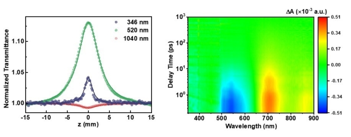
PdSe2 is regarded as a promising material to bridge the gap between graphene and MoS2 because of its bandgap varying from 1.3 eV (monolayer) to 0 eV (bulk), which has the potential for application in next-generation optoelectronic devices. Scientists observed the steady-state and transient photoresponse of trilayer PdSe2 films by the usage of nonlinear optical technique and ultrafast carrier dynamics system. Trilayer PdSe2 exhibits broadband nonlinear absorption behavior in the ultraviolet, visible, and near-infrared regions. Especially, PdSe2 exhibits well-performed saturable absorption at 346 nm and 520 nm, which indicates that PdSe2 can be used as a saturable absorber in ultrafast short-wavelength lasers.
Furthermore, based on its high modulation depth, a PdSe2-based visible light thresholder is proposed, whose function is to extract an undetectable pulse signal drowned in strong stochastic noise and thereby improve the signal-to-noise ratio. Pump-probe technique, along with transient absorption spectra, reveal the recombination lifetime of photo-generated carriers is approximately 100 ps, and the intrinsic recombination mechanism includes shallow defects-assisted Auger scattering and deep defects-assisted trap saturation.
This work proves that PdSe2 has the broadband optical response, the high modulation depth, and the fast response speed, which implies that PdSe2 is a promising material in broadband nano-optoelectronic devices.

Figure 1. Broadband nonlinear absorption and transient absorption spectra of PdSe2. (Image by SIOM)
Article Website:
https://doi.org/10.1002/adom.202101963
Contact:
WU Xiufeng
General Administrative Office
Shanghai Institute of Optics and Fine Mechanics, CAS
Email: xfwu@siom.ac.cn
Web: http://english.siom.cas.cn/